Prerequisites
- Install klink:
pip install klayout-klink(one command installs klink plus its Rust kernels). - KLayout running with the klink plugin loaded.
- This demo is a starter: it's already in the
klink init <proj>scaffold (example_template/digital/padframe_pnr_lvs.py), and needs a running KLayout session. The full commands are:python example_template/digital/padframe_pnr_lvs.py --port <session-port> # card mode python example_template/digital/padframe_pnr_lvs.py --port <session-port> --no-card # no-card mode # from a repo clone you can also run: python -m examples_klink.public.demos.digital.padframe_pnr_lvs --port <session-port> [--no-card]
padframe_pnr_lvs.py into 6 observable stages so each step of this reversed "card first, circuit yields" flow is visible on its own. In production you just run the one script -- the staged version is purely for teaching. It reuses the public 3-layer process and synthetic fitted-device library from the fit-a-device demo, so it owns zero device geometry of its own; the circuit is a 4-bit adder netted by an open logic synthesizer and remapped onto those synthetic devices (173 devices / 96 nets / 62 gates).1Synthetic circuit base: lint + layer advisor + flat placement
First lint the device netlist -- before any geometry exists, every structural mistake in a hand-written netlist (unknown instance, a terminal on two nets, an instance in no group, ...) is reported with its fix. Once lint passes, the layer-count advisor spreads out what each candidate stack would cost: fewer layers is always better (every extra layer is a real deposition / litho / via step) and the choice is yours. add4 routes comfortably on the public 3-layer stack, so that's what we use.
| Candidate stack | Routing layers | Signal layers | Core size |
|---|---|---|---|
public-3L | 3 | 2V + 1H | 920 × 1208 µm = 1.111 mm² |
example-7L | 7 | 2V + 2H | 920 × 984 µm = 0.905 mm² |
The advisor only reports the arithmetic; the candidate stacks themselves are example data (what your fab can actually build). In this stage's screenshot the device block is first placed flat with no band constraint (an 8×8 grid, row pitch 190 µm) -- used to measure the block footprint and size/position the card that comes next:
rep = lint_netlist(nl, device_terms=terms)          # structural lint; errors are fix-instructions
assert rep["ok"]
adv = layer_demand_report(nl, terms, [("public-3L", D.PUBLIC_PROCESS),
                                      ("example-7L", PUBLIC_MULTILAYER)])
rows, cols = derive_grid(len(nl["groups"]))          # 8 x 8
flat = eng.place_grid(nl, rows, cols, profile=P, row_pitch=rp)   # flat, no bands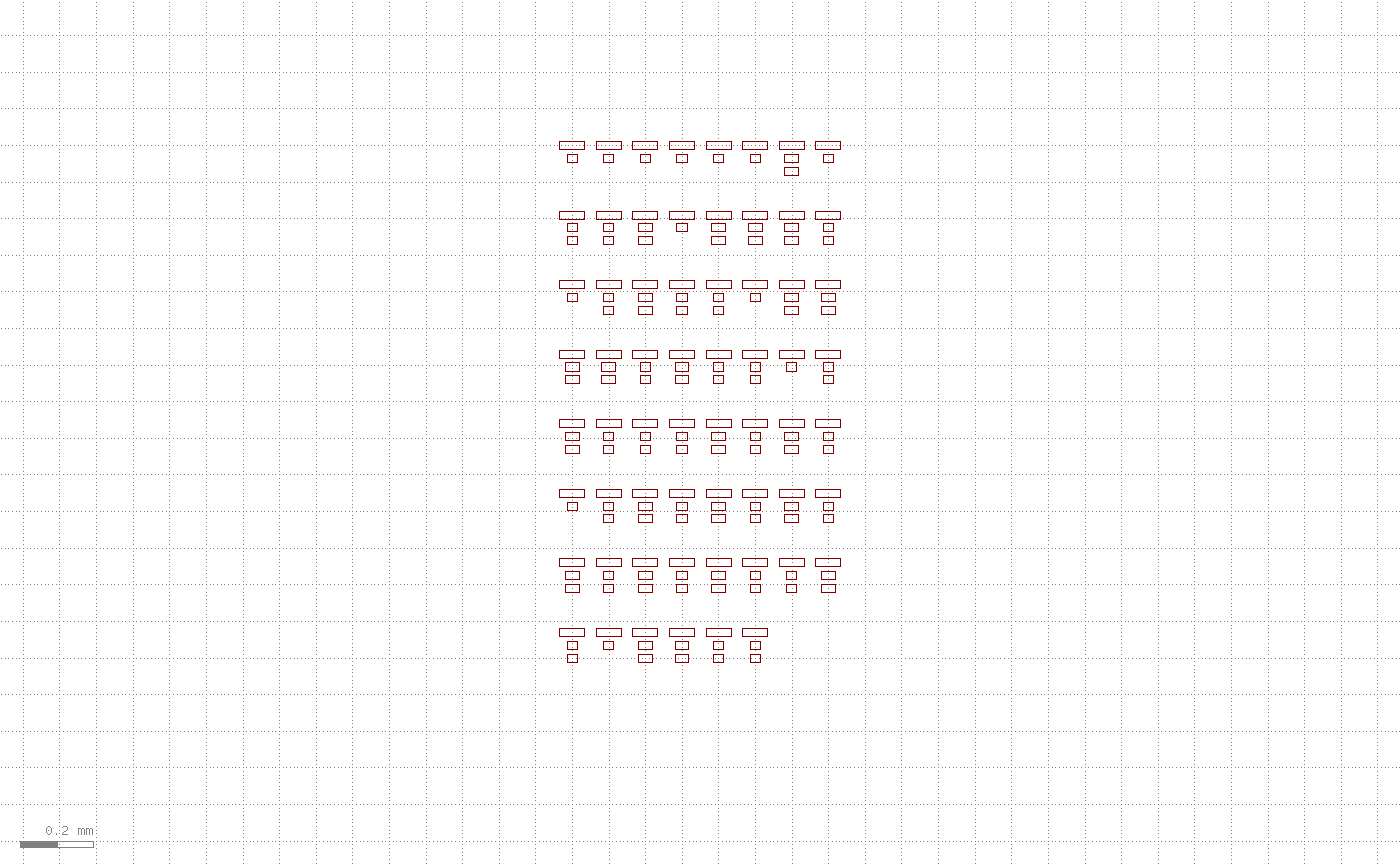
place_grid, 8×8 grid). This is the baseline for measuring the block footprint and positioning the card -- no card, no routing yet.2The user's probe card: fabricate a stand-in → harvest it back with pads_from_gds
This is the crux of the reversed order: the card exists first. To keep the demo self-contained we first write a stand-in probe-card GDS (20 pad squares in a ring on layer 106/0 -- pretend it came out of a drawer) and then harvest it back with pads_from_gds. In a real flow you skip the fabricate part and harvest your own card file directly:
from klink.routing.grid.pad_harvest import pads_from_gds

# Your real flow starts right here: pads_from_gds(YOUR_FILE, YOUR_CELL, YOUR_LAYER)
pads = pads_from_gds(CARD, "PROBE_CARD_20", "106/0", min_size_um=50.0)
# -> [{"id": "PAD00", "box_um": [...]}, ...]  20 pads
The card geometry is example data: pad 100×100 µm; the ring interior is wide enough for the block but only half its height -- exactly what drives the "half-in / half-out" case in stage ④. What you harvest is a plain pad table [{"id", "box_um"}, ...]; net assignment is a decision made on top, by a human or agent, afterwards.
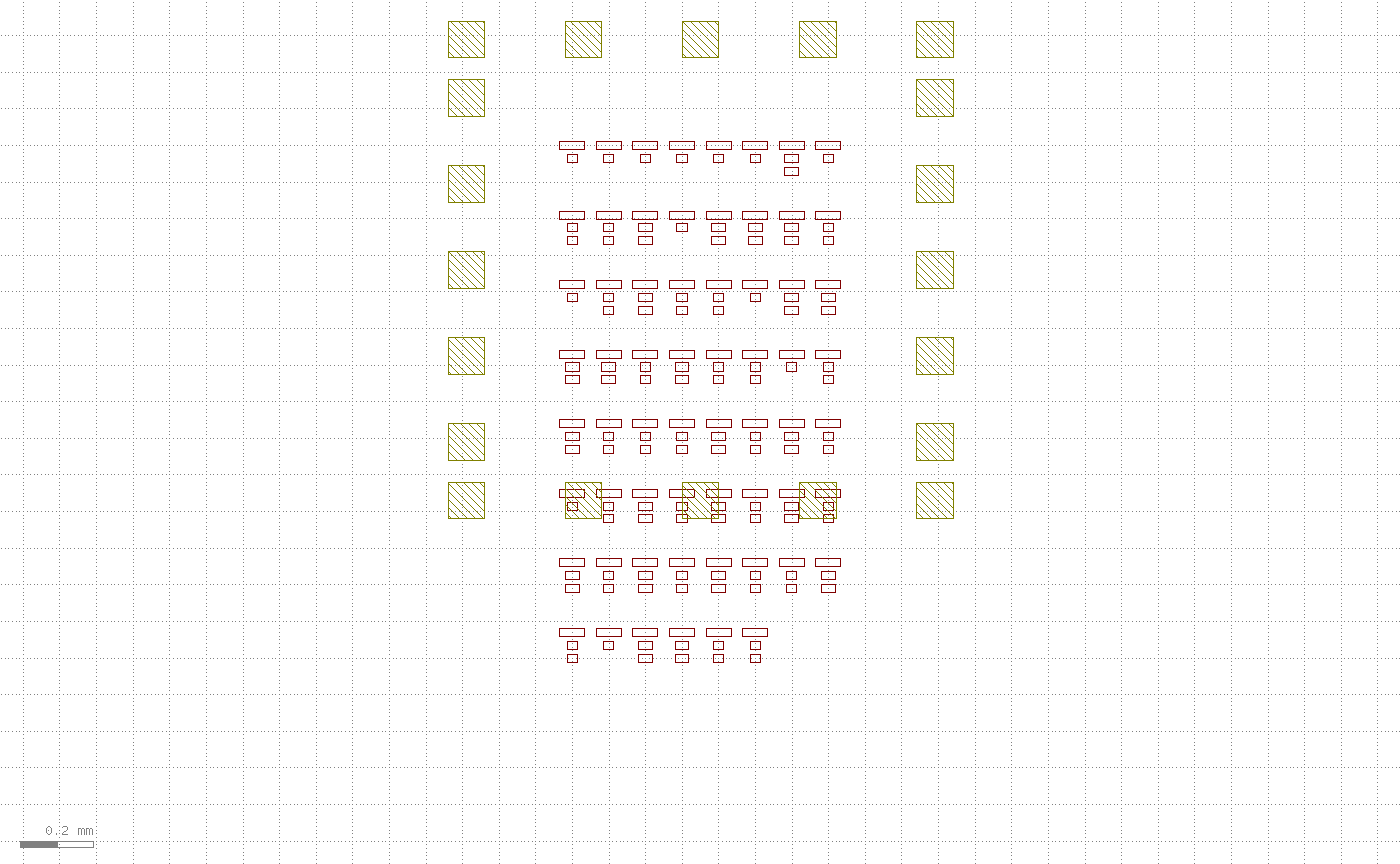
106/0): 5 left + 5 right + 5 top + 5 bottom. The interior can't fit the block's full height -- note the bottom pad row will cross the lower half of the block.3net → pad assignment table
Lay a plain table on top of the harvested pads: which net goes to which pad. The conventions here (edit freely): inputs on the left column + top row, outputs on the right column, GND on the top row (its tie rail derives above the block), VDD on the bottom-left corner pad (a clear corridor down the left margin to its rail below the block). 16 of the 20 pads are used (all 14 primary ports + VDD + GND); the remaining 4 redundant pads stay unused -- as on any legacy card.
def near(x, y):     # the harvested pad closest to a card point
    return min(pads, key=lambda p: (p["box_um"][0] - x) ** 2 + (p["box_um"][1] - y) ** 2)

for cy, net in zip(side_y, ["A[0]", "A[1]", "A[2]", "A[3]", "B[0]"]):
    near(ring_x1, cy)["net"] = net          # left column: 5 inputs
for cy, net in zip(side_y, ["S[0]", "S[1]", "S[2]", "S[3]", "COUT"]):
    near(ring_x2 - PS, cy)["net"] = net     # right column: 5 outputs
for cx, net in zip(row_x, ["B[1]", "B[2]", "GND", "B[3]", "CIN"]):
    near(cx, ring_y2 - PS)["net"] = net     # top row: inputs + GND
near(row_x[0], ring_y1)["net"] = "VDD" # bottom-left corner: VDD![Each pad labelled with a net name: left column A[0..3]/B[0], right column S[0..3]/COUT, top row B/GND/CIN, bottom-left VDD, and the bottom four labelled PAD16..19 as redundant unused](../assets/tutorials/padframe/step-03-assign.png)
PAD16..PAD19 keep their raw ids, marking them redundant pads with no net assigned.4Half-in / half-out placement
The card's bottom pad row crosses the device block. Since the card is fixed and the block is what yields, we forbid that horizontal band: place_grid(forbid_y_bands=[band]) pushes any device row that would hit it below the band. The first inner_rows rows stay inside the ring; the rest continue underneath, and routes thread between the bottom pads. This splits the whole block "half inside the pad ring, half outside" without any new placement engine.
band = (ring_y1 - CLR, ring_y1 + PS + CLR)          # bottom pad row + clearance
placement = eng.place_grid(nl, rows, cols, profile=P, row_pitch=rp,
                           forbid_y_bands=[band])   # rows hitting the band go below it
# measured: 85 devices inside the ring, 80 below it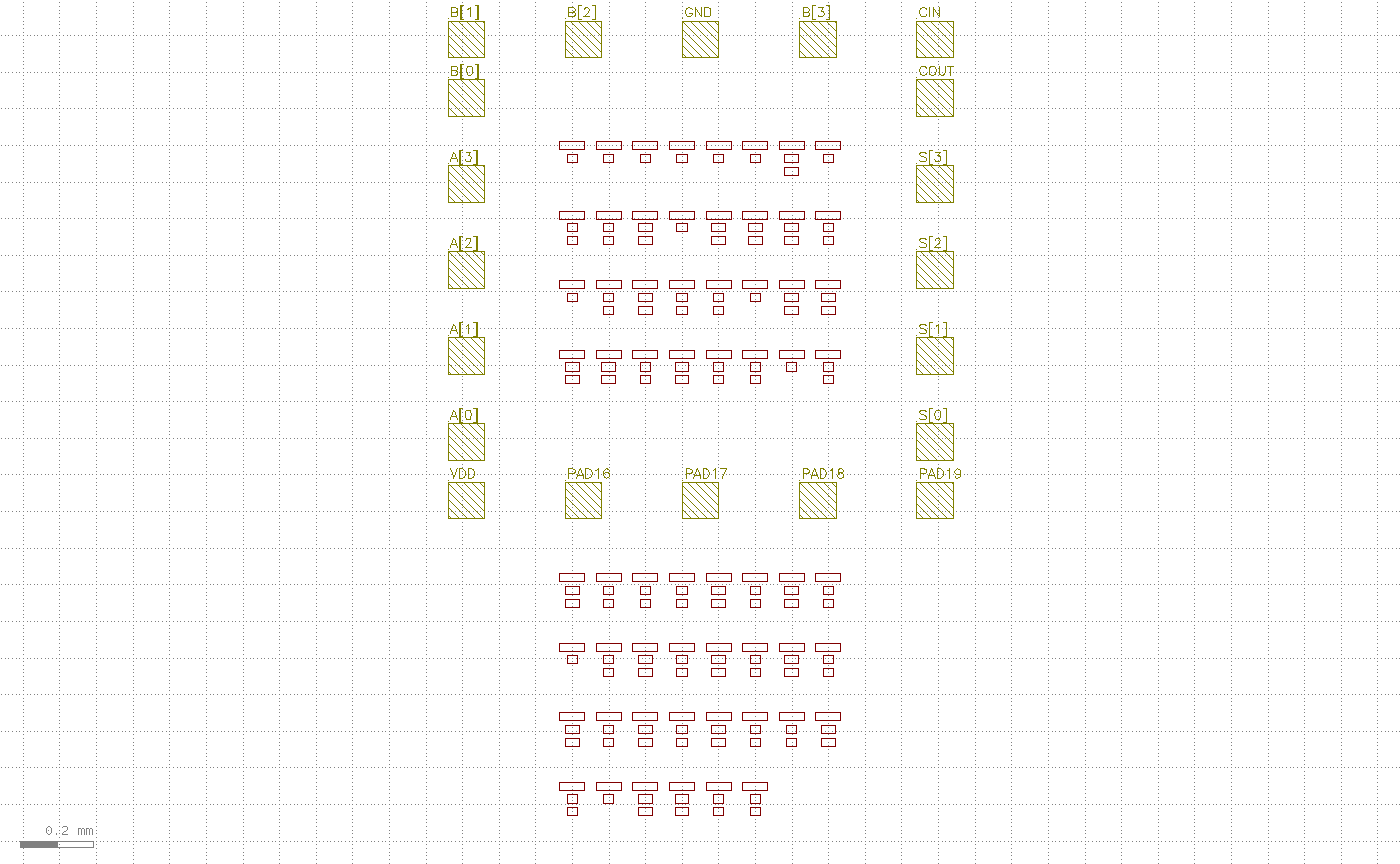
forbid_y_bands forbids the horizontal band the bottom pad row occupies: 85 devices stay inside the ring and 80 are pushed below it (compare to Step 3 -- the lower half shifts down as one, clearing the bottom pad row). The card stays put; the block yields.5Signal P&R + a region-split power grid, then the finished chip
One final call to route_and_draw_flexdr does three things at once: signal routing (faithful FlexDR on the track grid, avoiding the power grid), drawing the device PCells + traces + vias, and turning the assigned pads in io_pads into each net's own fixed metal + an extra route terminal (unused pads become hard keep-outs). The same forbidden band also splits the power grid: pdn_split_bands builds one PDN per region and bridges them with a single spine strap dropped through the widest pad-free gap of the bottom row -- power threads between the card's pads exactly like the signals do.
with KLinkClient(port=PORT).connect() as c:
    ok, info, _ = eng.route_and_draw_flexdr(
        c, "PUB_PADFRAME_ADD4", nl, placement, profile=P, layers=layers,
        vias=P.via_rules(), cut_layer=cut_layer, geom_path=D.GEOM, devices=DEVICES,
        use_rust=True, io_pads=IO, pdn_split_bands=[band])
    # -> routed 94/94, markers 0, 4.1s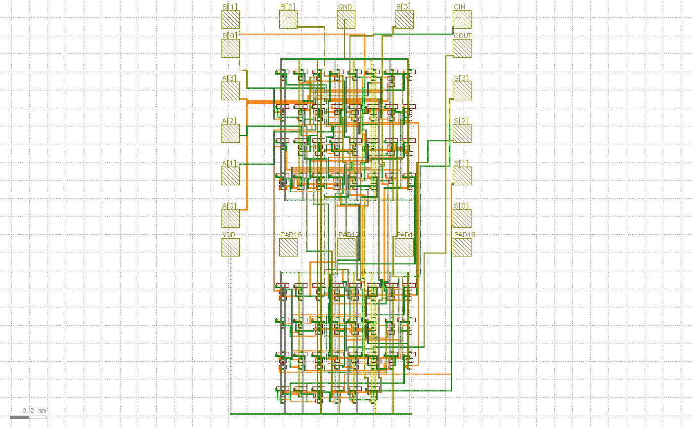
view.zoom_fit): routed 94/94 · markers 0. Both halves of the block are routed; signals reach the assigned pads around the ring; VDD runs from the bottom-left pad down the left corridor into the power grid, with the GND top-row rail above.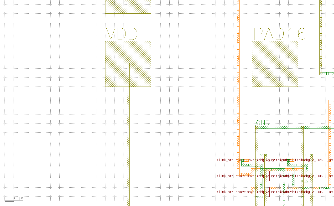
VDD pad drops a vertical strap corridor down its own centre to a power-grid tie rail -- a power pad needs a clean vertical lane to its net's rail; without one, route_and_draw_flexdr raises an error naming the conflict.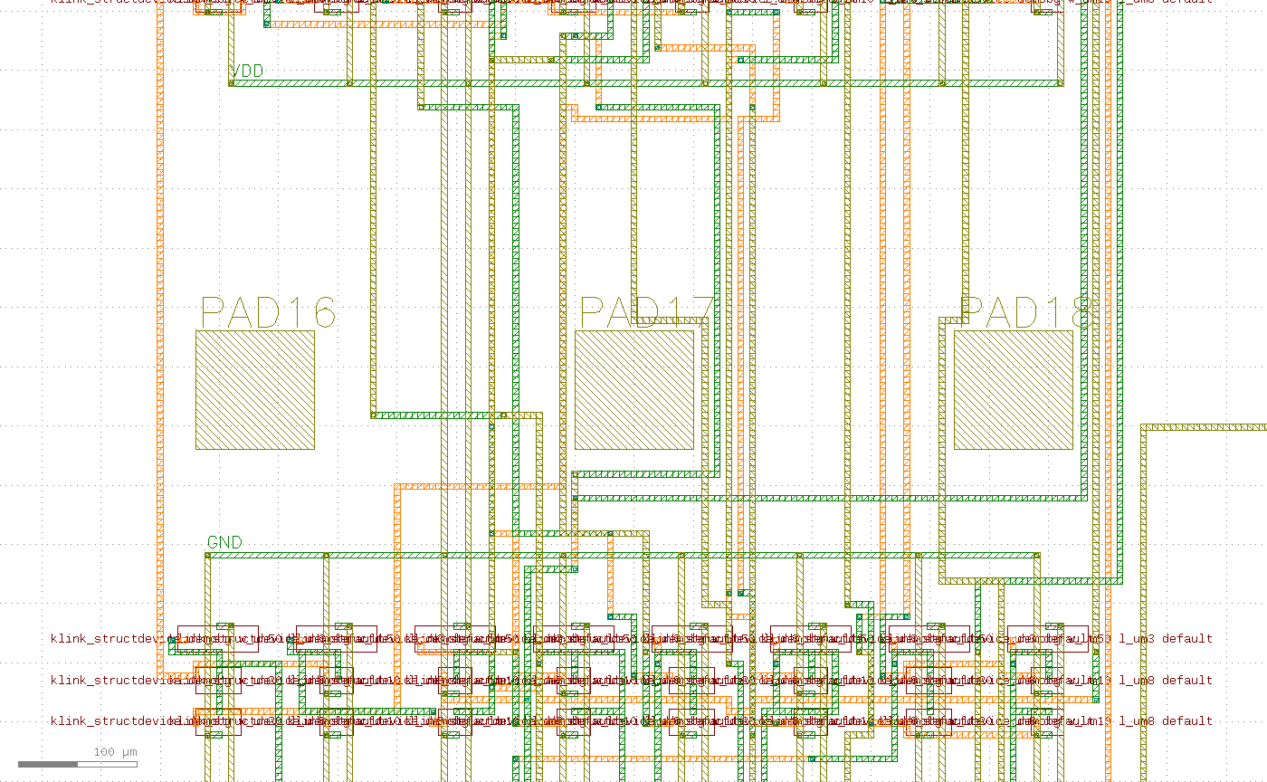
PAD16..18), bridging the in-ring PDN and the below-ring PDN -- power threads between the card's pads just like the signals.6No-card mode: every port becomes a bare stub
Add --no-card: no pads at all, and none are drawn. Every port leaves the block as a bare labelled trace -- spread_ports makes wire-end targets (draw=False: no box drawn; the route's own metal ends there, tagged with the net-name text). Inputs snap to the west edge, outputs to the east, both snapping to the routing-channel centres between device rows (so a stub never lands inside a device-row band and forces its horizontal run into a neighbouring channel). Power needs no stub at all: the PDN tie rails are auto-labelled VDD/GND -- bond/probe anywhere on the rail.
from klink.routing.grid.pad_harvest import spread_ports

IO2 = {"pad_layer": "106/0", "text_size_um": 15.0,
       "pads": (spread_ports(BB, INPUTS,  side="W", size_um=P.wire_width_um,
                             clear_um=120.0, prefix="IN",  snap=chan)     # inputs west
                + spread_ports(BB, OUTPUTS, side="E", size_um=P.wire_width_um,
                             clear_um=120.0, prefix="OUT", snap=chan))}   # outputs east
ok2, info2, _ = eng.route_and_draw_flexdr(
    c, "PUB_PADFRAME_ADD4_NOCARD", nl, flat, profile=P, layers=layers, ...,
    io_pads=IO2, pdn_split_bands=None)      # -> routed 94/94, markers 0, 3.6s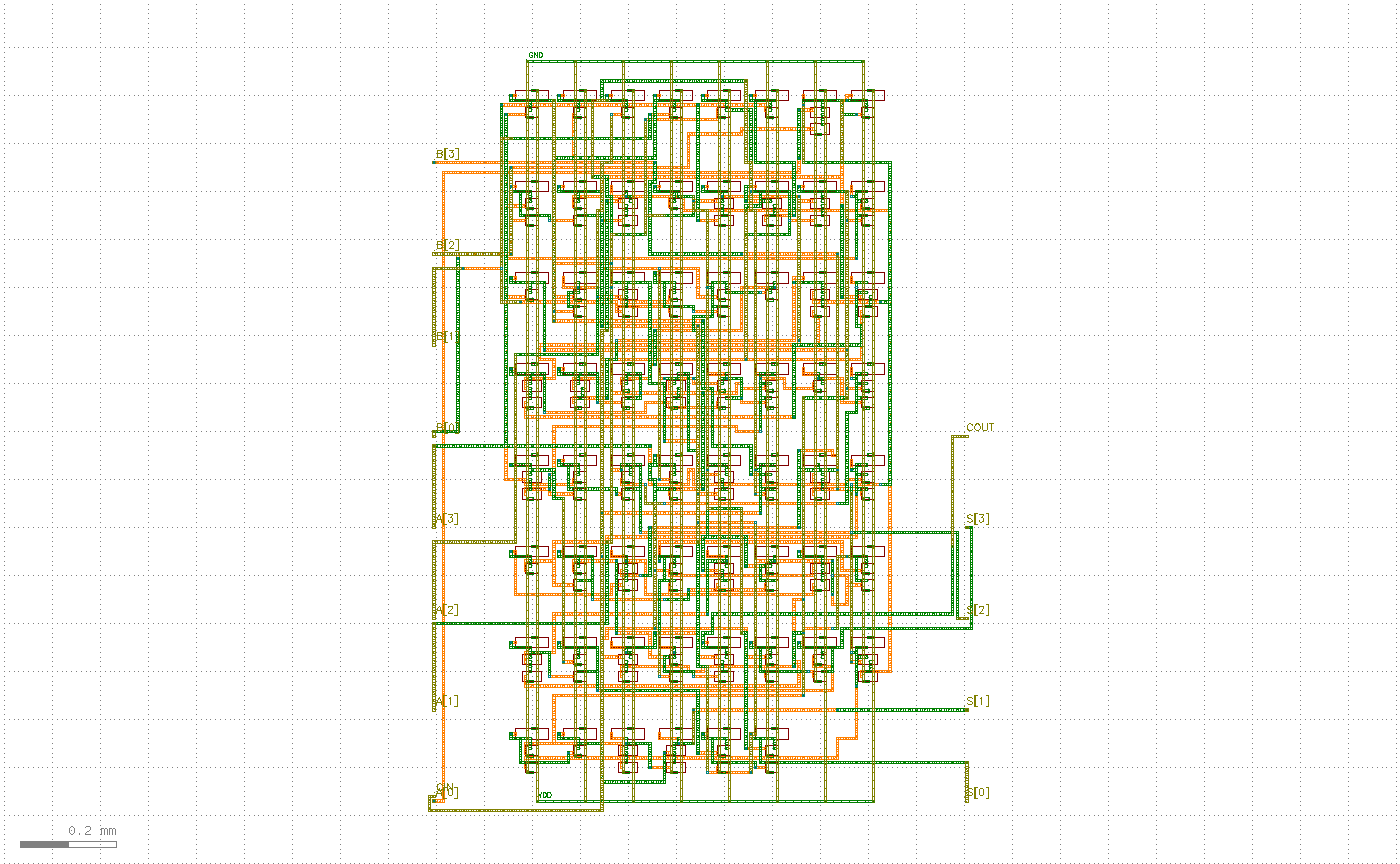
--no-card finished: routed 94/94 · markers 0. No pad ring -- inputs (A[*]/B[*]/CIN) on the west, outputs (S[*]/COUT) on the east, all bare labelled stubs; power sits on the auto-labelled PDN tie rails.![Zoom on the west edge: net names like A[1] and CIN sit at the end of a trace, where the route simply ends, with no pad box](../assets/tutorials/padframe/step-06-detail-stub.png)
A[1] and CIN sit at the trace end -- the wire end is the port, no pad box is drawn (draw=False). The labels tell you where to hook up your own pads later.Verify: each mode's own live LVS
As in every tutorial here, screenshots are for people, not proof of done. This demo's bar is a live LVS match=True in each mode, plus a positive per-pad proof: every assigned pad/stub's metal must sit on the same extracted net as its net's device terminals, and every unused pad must touch no net. The real numbers from this run (session 8767, Rust kernel):
| Mode | routed | DRC markers | LVS ok | LVS match | devices | per-pad proof | time |
|---|---|---|---|---|---|---|---|
| card (with card) | 94/94 | 0 | True | True | 173 | 16 connected + 4 isolated | 4.1s |
--no-card | 94/94 | 0 | True | True | 173 | 14 connected + 0 isolated | 3.6s |
# card mode
[PUB_PADFRAME_ADD4]        LVS ok=True match=True devices=173
[PUB_PADFRAME_ADD4]        pad proof ok=True connected=16 isolated=4
# --no-card mode
[PUB_PADFRAME_ADD4_NOCARD] LVS ok=True match=True devices=173
[PUB_PADFRAME_ADD4_NOCARD] stub proof ok=True connected=14 isolated=0
Both modes' match is True, both have 0 DRC markers, and both pass the per-pad/stub proof -- that's what "the padframe is done" rests on. Card mode: all 16 assigned pads CONNECTED, all 4 redundant pads isolated. No-card mode: all 14 bare stubs CONNECTED (power takes no stub -- it lives on the PDN rails).
Next steps
Copy padframe_pnr_lvs.py and edit its pad table (pad size, positions, the net→pad convention) to describe your own card; edit PUBLIC_PROCESS / PUBLIC_MULTILAYER for your own stack -- the flow is unchanged, klink ships only the mechanism. To first understand how the device itself is fitted from example geometry into a parametric PCell before P&R, see the companion Step-by-step: fit a device → P&R → LVS. For measured numbers on all the public demos, see the Examples page · Probe-card padframe.