Prerequisites
- Install klink:
pip install klayout-klink(one command installs klink plus its Rust kernels -- no third-party scientific libraries needed). - KLayout running with the klink plugin loaded (RPC port defaults to
8765). - Scaffold a project and enter it:
klink init nano-demo && cd nano-demo-- the full script ispython example_template/nanodevice/hallbar.py --live --port <session-port>. In a repo checkout the equivalent ispython -m examples_klink.public.demos.nanodevice.hallbar --live --port <session-port>.
hallbar.py into 7 observable stages so each step of what's drawn, marked, and why is visible on its own. In production you'd usually still write geometry with one shape.insert_many batch call (see the batch-RPC rule in this repo's CLAUDE.md) -- the staged version here is purely for teaching.1Create the cell + plan the layers
Start with a disposable cell, then ensure every layer this device needs. The Hall bar is a fully offline, self-contained device -- it carries its own layer numbers and reads no PDK:
| Layer | Purpose |
|---|---|
1/0 | Device layer (mesa / conducting channel) |
10/0 | Metal layer (ohmic contacts + probe pads) |
6/0 | Label layer |
12/0 | Route layer (fanout traces, written after routing) |
999/99 | klink's reserved Port marker layer |
999/1 | klink's reserved Anchor marker layer |
from klink import KLinkClient

with KLinkClient(port=PORT).connect() as c:
    cell = c.cell_create("NANODEVICE_HALLBAR_TEST")["cell"]
    device_li = c.layer_ensure(1, 0, name="NANODEVICE_DEVICE")["layer_index"]
    metal_li  = c.layer_ensure(10, 0, name="NANODEVICE_METAL")["layer_index"]
    label_li  = c.layer_ensure(6, 0, name="NANODEVICE_LABEL")["layer_index"]
    route_li  = c.layer_ensure(12, 0, name="KLINK_ROUTES")["layer_index"]
view.zoom_box framed on where the device will sit; nothing is drawn yet).2Draw the mesa / channel
The mesa is a centered rectangular conducting channel, sized from HallBarSpec's bar_length_um / bar_width_um (144 × 8 µm by default). Full coordinate arithmetic lives in example_template/nanodevice/hallbar.py; here's just the write call:
c.shape_insert_boxes(cell, layer_index=device_li, boxes_um=[mesa_bbox_um])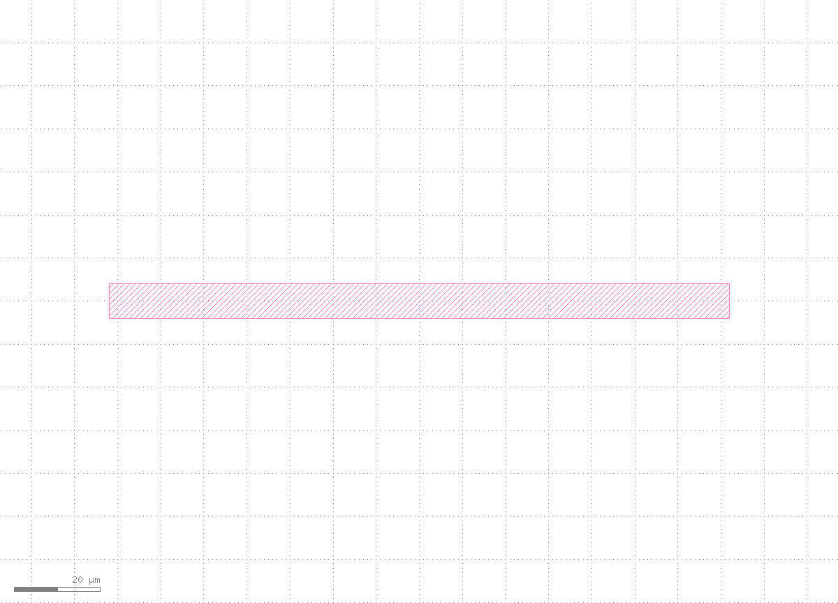
1/0).3Draw the ohmic contacts
Three narrow contact stubs stick out from each of the mesa's top and bottom edges (contact_count=6 in this example). Each contact's inner end sits exactly on the mesa edge -- that's where the Port will later fire from.
c.shape_insert_boxes(cell, layer_index=metal_li, boxes_um=contact_bboxes_um)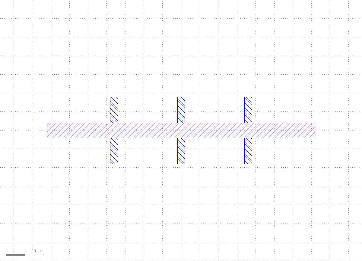
10/0), extending outward from the mesa edge.4Draw the probe pads
Each contact gets a matching large probe pad; pad-to-mesa distance is set by pad_gap_um -- this is the "array pitch vs. probe-pad pitch are different scales" case from this repo's CLAUDE.md. The gap between a contact and its pad is exactly what stage ⑥ will route.
c.shape_insert_boxes(cell, layer_index=metal_li, boxes_um=pad_bboxes_um)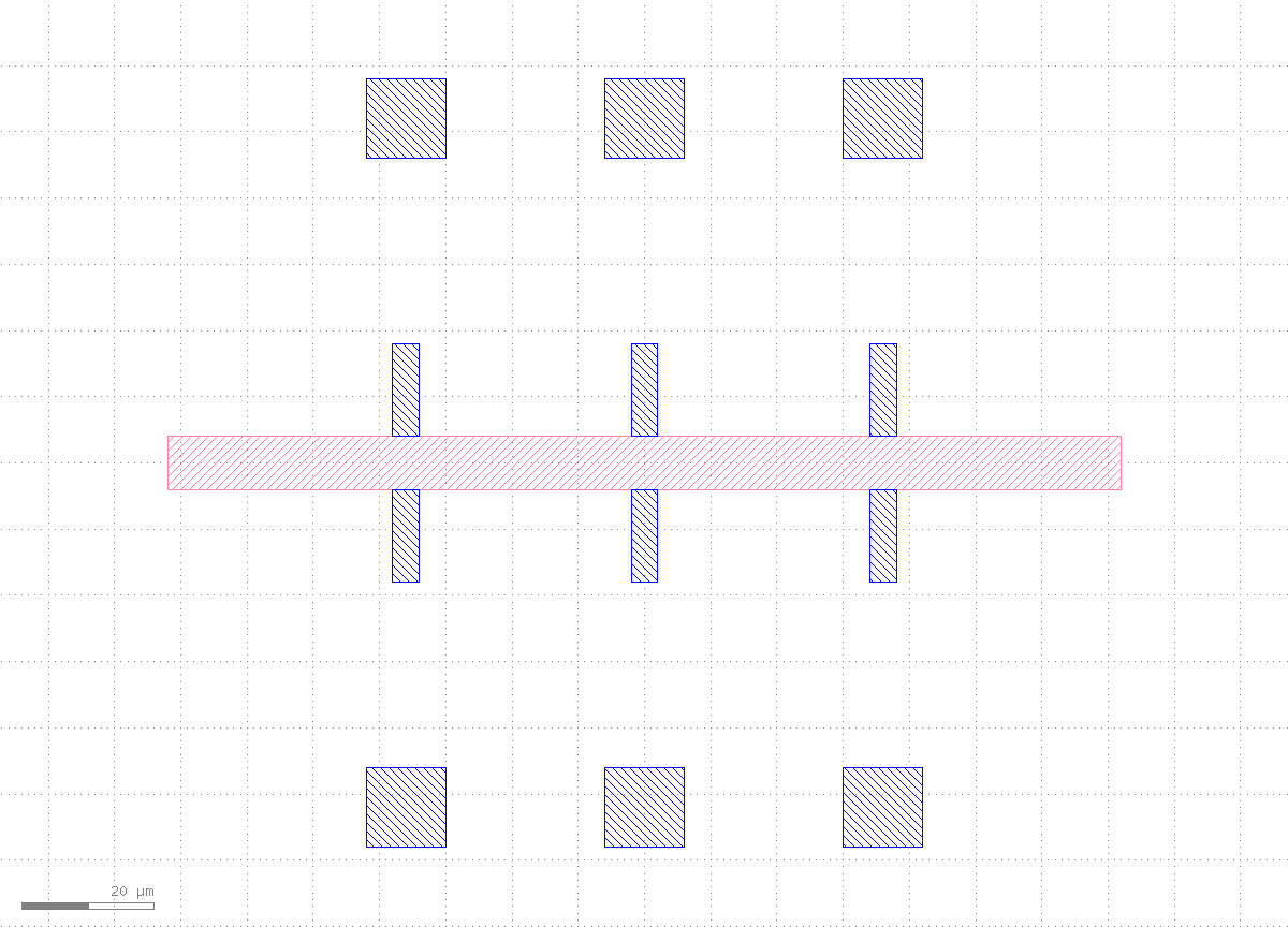
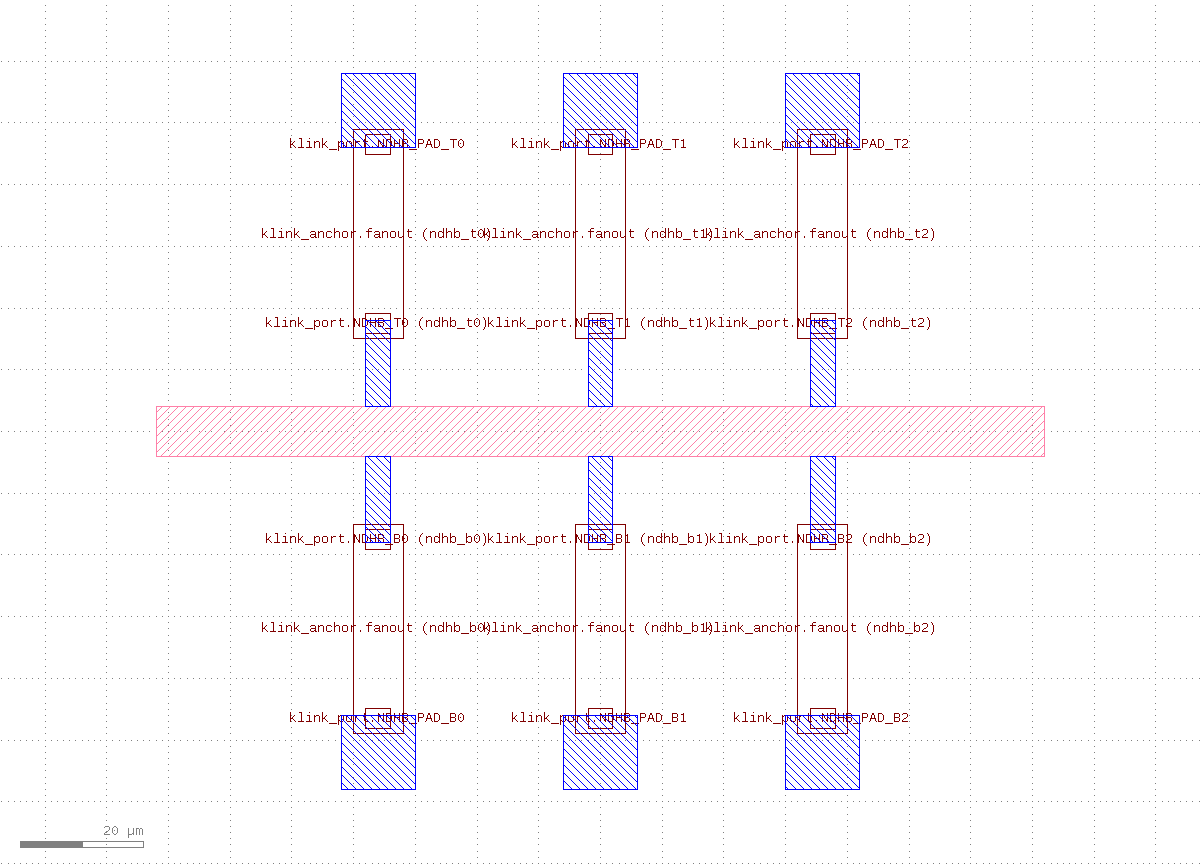
10/0) -- still no wiring between contacts and pads at this point.5Mark Port + Anchor intent
This is the geometry-first pivot: instead of drawing the wires directly, you mark "a wire needs to leave from here" (Port) and "the wire must pass through this region" (Anchor waypoint_region). Each contact is an electrical Port carrying a real net; each pad is a candidate_sink Port -- a candidate endpoint with no net assigned yet:
c.call("port.mark", {
    "cell": cell, "layer": "999/99", "name": "NDHB_T0",
    "center_um": [-36, 18], "orientation": 90, "width_um": 4,
    "net": "ndhb_t0", "target_layer": "12/0",
})
c.call("anchor.mark", {
    "cell": cell, "layer": "999/1", "id": "NDHB_T0_WAYPOINT",
    "kind": "waypoint_region", "center_um": [-36, 32],
    "width_um": 8, "height_um": 34, "net": "ndhb_t0",
})
6Route the fanout
Once everything is marked, call klink's tapered-hybrid routing backend: planning happens client-side in Python (a visibility graph + Dijkstra, no rasterization), and the result is written back to layer 12/0 with one batched RPC:
from klink.routing.backends.geometric.tapered_segments import (
    route_tapered_hybrid_many, commit_tapered_hybrid_many,
)

pairs = [{"net": contact["net"], "source": contact, "target": pad,
          "route_layer": "12/0"} for contact, pad in zip(contact_ports, pad_ports)]
route_result = route_tapered_hybrid_many(pairs, anchors=anchor_marks)
assert route_result["ok"]
commit_tapered_hybrid_many(c, cell, route_result, route_layer="12/0", clear=True)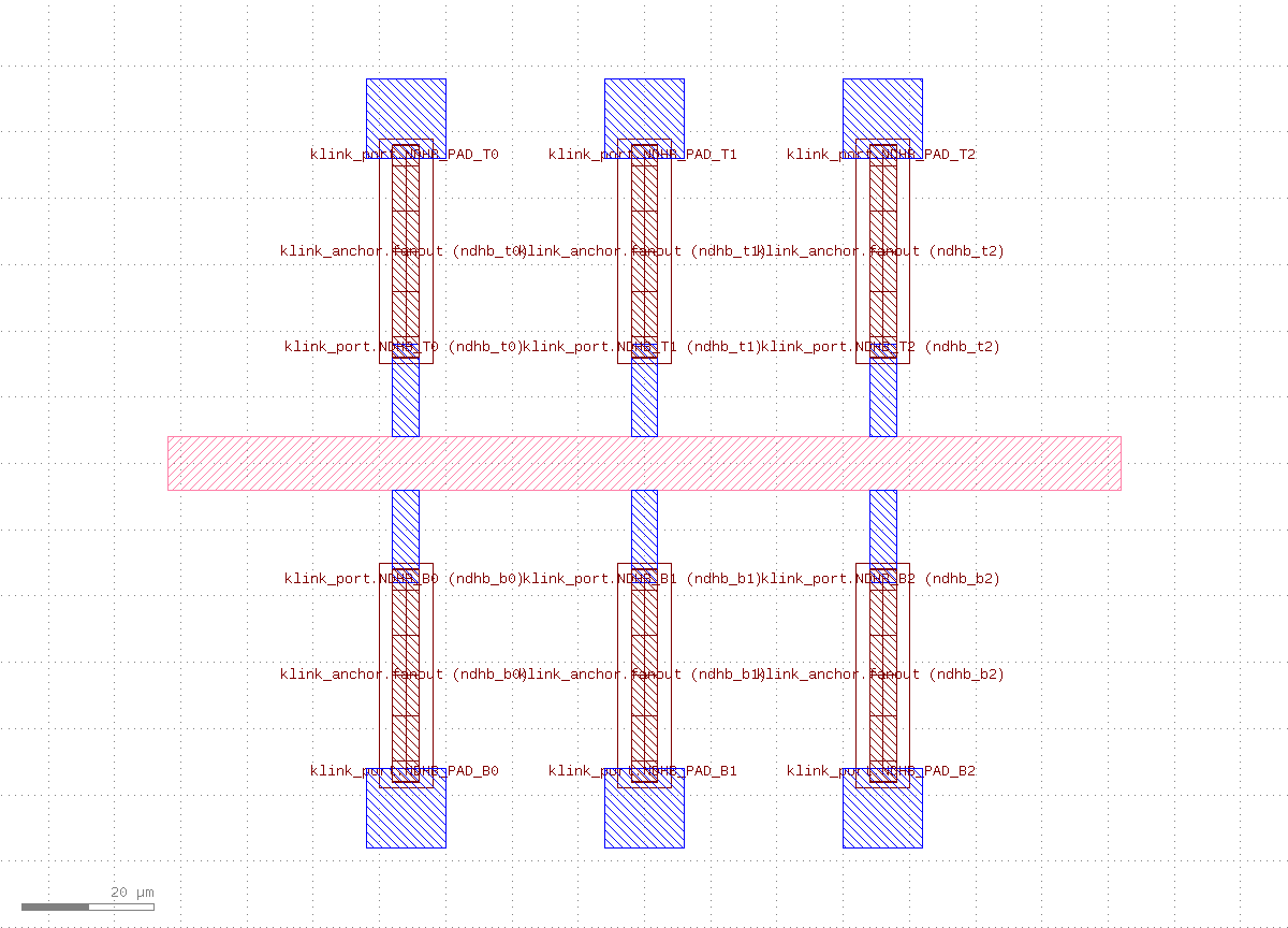
7Finish: label + overview/detail
Last, write the device name label, then look at the whole chip and one detail:
c.shape_insert_text(cell, "NDHB", layer_index=label_li,
                     position_um=[-72, 10], size_um=3.0)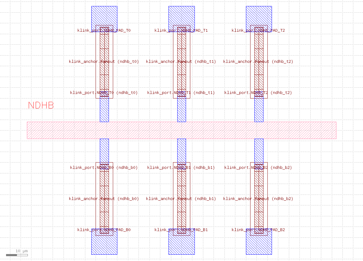
view.zoom_fit): mesa + 6 contacts + 6 traces + 6 pads + label.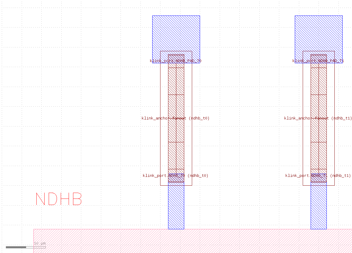
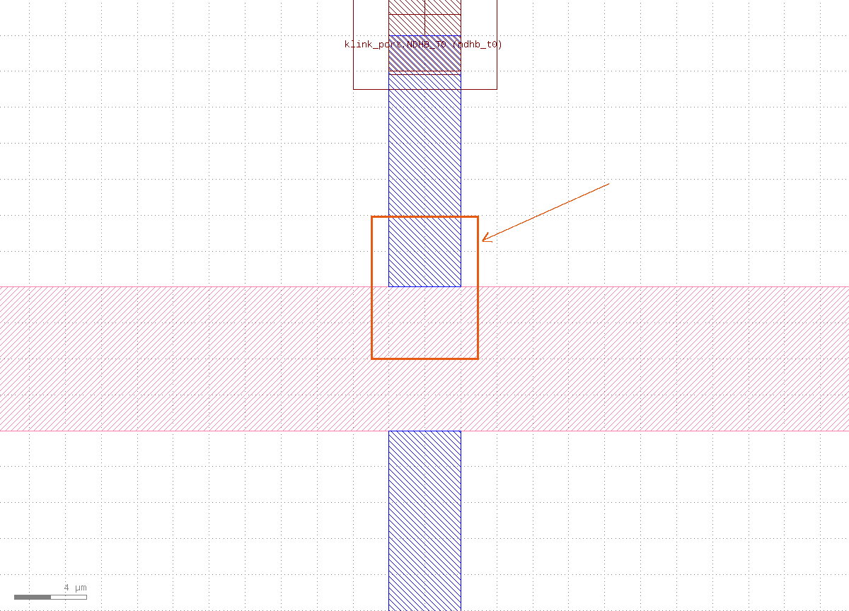
Verify, don't just look
As the tutorials home page says: screenshots are for people, not proof of done. Here's the actual routing report from this run:
{
  "ok": true,
  "route_count": 6,
  "obstacle_hits": 0,
  "sibling_overlaps": 0
}
ok=true with zero obstacle_hits and zero sibling_overlaps means all 6 fanout traces avoid each other and any obstacle layer -- that's what "routing is done" actually rests on, not "it looks connected."
Next steps
Edit the HallBarSpec parameters in example_template/nanodevice/hallbar.py to your own sizes (contact count, pad spacing, layer numbers), rerun with --live, and confirm the routing report still says ok=true. From there, decide whether you need writefield obstacle avoidance (EBL scenarios) or a drc.run pass. For more on offline devices see Core concepts & tutorials · Offline device tutorial; the full Port/Anchor field reference is in the MCP reference.